
Overview
Researchers, led by Peter Delfyett at the University of Central Florida College of Optics and Photonics (CREOL), have demonstrated a silicon-based optical communication link that combines two multiplexing technologies to create 40 optical data channels that can simultaneously move data. The new chip-scale optical interconnect can transmit about 400 GB/s which is equivalent to roughly 100,000 streaming movies. This could improve data-intensive internet applications from video streaming services to high-capacity transactions for the stock market.
This new method achieves 40 channels by combining a frequency comb light source with an optimized mode-division multiplexer. The source is based on a new photonic crystal resonator developed by the National Institute of Standards and Technology (NIST) while the multiplexer was designed by the researchers at Stanford University. Each channel can be used to carry information much like different stereo channels, or frequencies, transmit different music stations.
In addition to improving data transmission across the internet, this new technology could also be used to make faster optical computers. This could provide the high levels of computing power needed for artificial intelligence, machine learning, large-scale emulation and other applications.
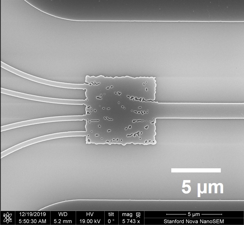
he researchers designed and optimized a mode-division multiplexer that transforms each of the 10 wavelengths into four new beams that each have different shapes. This fourfold increase in data capacity creates 40 channels. Image Credit: Kiyoul Yang, Stanford University
Multiple Light Dimensions
The researchers created the optical link using tantalum pentoxide (Ta2O5) waveguides on a silicon substrate fabricated into a ring with a nanopatterned oscillation on the inner wall. The resulting photonic crystal micro-ring resonator turns a laser input into ten different wavelengths. They also designed and optimized a mode-division multiplexer that transforms each wavelength into four new beams that each have different shapes. Adding this spatial dimension enables a fourfold increase in data capacity, creating the 40 channels.
Once the data is encoded onto each beam shape and each beam color, the light is recombined back into a single beam and transmitted to its destination. The wavelengths and beam shapes are then separated so that each channel can be received and detected independently, without interference from the other transmitted channels.
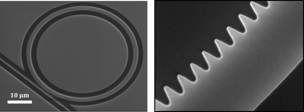
The ring-shaped photonic crystal resonator (left) features a nanopattern inside (right) that splits a selected resonant mode for comb generation. Images taken with scanning electron microscopy. Image Credit: Su-Peng Yu, NIST
Inverse Design
The researchers used a computational nanophotonic design approach called photonic inverse-design to optimize the mode division multiplexer. This method provides a more efficient way to explore a full range of possible designs while offering smaller footprints, better efficiencies and new functionalities.
Tests of the new device matched well with simulations and showed that the channels exhibited a low crosstalk of less than -20 dB. Using less than ~10 dBm of received optical receiver power, the link performed error-free data transmission in 34 out of the 40 channels using a PRBS31 pattern, a standard used to test high-speed circuits under stress.
The researchers are now working to further improve the device by incorporating photonic crystal micro-ring resonators that produce more wavelengths or by using more complex beam shapes. Commercializing these devices would require the full integration of a transmitter and receiver chip with high bandwidth, low power consumption and a small footprint. This could enable the next generation of optical interconnects for use in data-center networks.
Related Links
Paper: Photonic crystal resonators for inverse-designed multi-dimensional optical interconnects